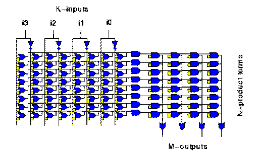
Fig. 1.1 PLA
In the particular case, we have a K-inputs, N-product terms and M-outputs PLA. Each small yellow square in the AND-plane represents a memory cell which allows us to construct product-terms from a selection of the input signal (and their complements). The memory cells in the OR-plane allow to activate a product-term as an input of a given subset of the output functions. PLAs provide a fast implementation of large product-terms and can be used as a logic block within a FPGA by linking them with programmable interconnect as with LUTs. On the other hand there exist some interesting functions (parity, arithmetic..) for which the number of product-terms can be exponential in the number of inputs. It is interesting to compare the structure of a PLA with a ROM memory array (or a LUT, see Fig 1.2 ).
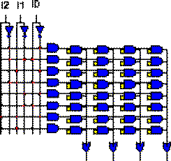
Memory (LUT)
Topologically, both structures are identical. The only difference is that the decoder (AND-plane) of the ROM enumerates all possible minterms, while the AND-plane of the PLA only realizes a limited set of them. Finally, Fig 1.3 illustrates a Programmable Array Logic device (PAL) having the OR-plane fixed and the AND-plane programmable.
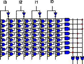
Fig 1.3 PAL
In[1], Brown and Rose give a complete tutorial of the commercially available Field-Programmable Logic Devices (FPD), providing a clear classification of them in the three main categories: simple PLDs, complex PLDs and FPGAs.
1.2 PLA-based FPGAs
In[2] Kouloheris and El Gamal investigate experimentally the tradeoff between the area of a PLA-based FPGA and its cell granularity. They propose PLAs as an area-efficient alternative to LUTs due to the two following considerations:- a LUT with much more than 4 inputs is prohibitively large because of its exponential growth in size with the number of inputs;
- it has been found that, on average, the functions mapped into the LUTs used considerably fewer product-terms than the LUT capacity;
- 1 output cells are the smallest from K=2 to K=4;
- 2 output cells are the smallest from K=4 to K=7;
- 3 output cells are the smallest beyond K=7;
1.3 PLA-based FPGA vs. LUT-based FPGAs
Kouloheris and El Gamal compared the smallest LUT implementations with the smallest PLA implementations, considering the same programming technology, namely EPROM cells. The total-area for the PLA cell implementation ranges from 80% to 130% of the LUT one (without considering the ECC benchmarks which produce very bad results, namely 300% worse). A disadvantage of these PLA-based implementations is that they dissipate static power. On the other hand, they claim that the PLAs give in average 25% fewer wiring tracks and 40% fewer levels of logic, which would lead to a better performance. Still, it should be considered that a reduction in logic levels produce in general an increasing of the average fanout per cell output which can bound the possible performance gain.1.3 PLA Area Optimization Technique
Statistical analysis show that on average only about half of the inputs are involved in any of PLA product-term. This suggest that a fixed product-term folding could be used to reduce the PLA size (Fig 1.4)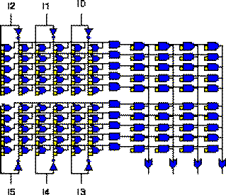
Fig. 1.4 PLA Area Optimization: Product-term Folding
Moreover, the fact that only about 10% of the product terms are shared between outputs leads to fix the OR-plane as in PALs. (Fig 1.5)
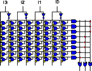
Fig. 1.5 PLA Area Optimization: Fixed OR-Plane
1.4 A Commercial PLA Device: ALTERA 9000
The general architecture of tha ALTERA 9000 is shown in Fig 1.6a: the FastTrack interconnect provide the communication among the Logic Array Blocks (LABs) and the I/O cells.
Fig. 1.6a ALTERA 9000: General Architecture
Each LAB contains 16 macrocells having the structure illustrated in Fig. 1.6b: a programmable AND-plane feeds an OR gate and a flip-flop.
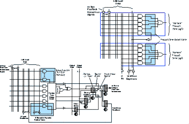
Fig. 1.6b ALTERA 9000: Logic Array Block
2 Universal Logic Module
2.1 ULMs and FPGAs
Universal Logic Modules (ULMs) are logic block capable of realizing all functions of a fixed number of variables assuming that permutations and negations of variables are provided outside these blocks. Old research on ULMs [3] and new work on FPGAs have not been related until recently, when studies started appearing about the usefulness of ULMs as logic blocks in FPGAs[4,5]. ULMs are defined as blocks with m general purpose inputs that can realize any function up to n inputs with n < munder the assumption that permutations and negations of signals are generated cost-free outside the logic block. This assumption virtually holds for FPGAs.2.2 Equivalence Classes of Boolean Functions
The set of Boolean functions of n variables can be divided into equivalence classes considering the following operations:- input inversion (N)
- input permutation (P)
- output inversion (N)
| Function | N | NP | NPN |
| 0 | |||
| 1 | |||
| a | a | a | a |
| a' | |||
| b | b | ||
| b' | |||
| ab | ab | ab | ab |
| a'b | |||
| ab' | |||
| a'b' | |||
| a+b | a+b | a+b | |
| a+'b | |||
| a+b' | |||
| a'+b' | |||
| a@b | a@b | a@b | a@b |
| a'@b' | |||
| 16 | 5 | 4 | 3 |
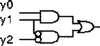
Fig. 2.1 An Example: ULM.2
The following table shows a set of possible assignments for y0, y1, y2 realizing all the 2-input functions.
| Function | y0 | y1 | y2 |
| 0 | 0 | a | 1 |
| 1 | 1 | a | 0 |
| a | 1 | a | 1 |
| a' | 0 | a | 0 |
| b | b | a | b' |
| b' | b' | a | b |
| ab | b | a | 1 |
| a'b | 0 | a | b' |
| ab' | b' | a | 1 |
| a'b' | 0 | a | b |
| a+b | 1 | a | b' |
| a+'b | b | a | 0 |
| a+b' | 1 | a | b |
| a'+b' | b' | a | 0 |
| a@b | b' | a | b' |
| a'@b' | b' | a | b |
2.3 Replacing LUTs with ULMs for FPGAs?
Each computational block of a FPGA can be implemented with a ULM instead of a LUT. However, observe that to compensate the lack of internal programmability, a ULM has always more inputs than an equivalent LUT. The following table illustrates the relationship between the number of input of the classes of functions to realize and the minimum number of inputs of the corresponding ULMs:| n | ULM Inputs |
| 2 | 3 |
| 3 | 5 |
| 4 | 8 |
| 5 | 13 |
| 6 | 21 |
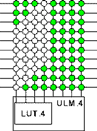
Fig. 2.2 ULM Input and Switches