
By now, you would have known how to enter and simulate your designs using Spectre. The next step in the process of making an integrated circuit chip is to perform a layout. What is a layout? A layout is basically a drawing of the masks from which your design will be fabricated. Therefore, layout is just as critical as specifying the parameters of your devices because it determines whether yours is a working design or a flop!
There are 2 ways to doing a layout: manual and automated. Manual layout usually enables the designer to pack his devices in a smaller area compared to the automated process but it is more tedious. The automated process, on the other hand, is done using standard cells and usually takes more real estate space but it is much faster. In this tutorial, you will learn how to perform MANUEL LAYOUTS ONLY and a simple inverter layout will be shown. You should know that for the purposes of this course, you are required to know how to design manual layouts, even though Cadence can accommodate either manual or automated layouts.
Before we get into the layout, first you need to understand the design rules for layout. The design rules that we will be using are the MOSIS Scalable CMOS Rules. Design rules gives guidelines for generating layouts. They dictate the spacings between wells, sizes of contacts, minimum spacing between a poly and a metal layer and many other similar rules. Design rules are essential to any successful layout design, since they account for the various allowances that need to be given during actual fabrication and to account for the sizes and the steps involved in generating masks for the final layout. The design rules that we will be using can be obtained from the following link on MOSIS Layout Design Rules. Note that the layout is very much process-dependent, since every process has a certain fixed number of available masks for layout and fabrication. For the case of this tutorial, we are using an AMI 0.6u CMOS process, which is a nwell process and supports two poly and three metal layers.
Before we proceed any further, please make sure that your present library is associated with a techfile. If you had followed this tutorial for your design of an inverter, then you might have already associated a techfile when you created a library ESE570 in the first place. Otherwise, you can still do it, by clicking on the middle button by placing the mouse on the library name in the library manager window. There is an option for "Attach Tech Library". Once you choose that option, click on AMI 0.6u C5N(3M,2P,high-res) as your process.
1. Create a layout cellview of the cell. Here we will create a layout
for the inverter cell.
In the library manager window, click on the File
-> New -> CellView. Choose CellName as inverter and View
Name as layout. Then click on the OK
button. An empty layout editor window will pop-up along with a LSW
window. The LSW window will show all the layers such as nwell, pwell,
active, etc. for the given process. An alternate way to open the layout
editor window is to type “layout” into the View box of the inverter cell in the
Library Manager window. A “Create
New File” window will pop-up.
Change the Tool item from “Composer-Schematic” to “Virtuoso” and make
sure the View Name is “layout”. If
not, manually change this by typing this in.
If the LSW window is blank, then there is an error (Follow this link to solve the problem).
The LSW window should look something like this:

If you don't see the above (not necessary to be in the above order) you will need to set the mask layers manually. To do this, go to Edit -> Set Valid Layers and select/deselect the masks. Make sure that you at least have the following masks in your LSW window.
nwell, nselect, pselect, nactive, pactive, poly, elec, metal1, metal2, metal3 (all dg's) & metal1, metal2, metal3 (pn's).
3. Since we are using the AMI 0.6u technology, we only have an nwell process to use. Thus, the substrate will be a p-type substrate. We can always assume that the background is a p-subtrate. Now we will create a pmos transistor first. To do that, we need an nwell layer in which the pmos transistor will be formed.
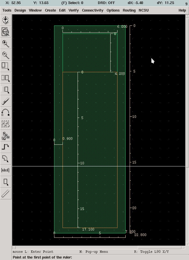
Note: You may adjust the minimum distance between the grids. In order to do it, in the Virtuoso Layout Editing window select Options --> Display. A new window will open. On that window, change "Minor Spacing" to a value that you want. In order to work efficiently, you can adjust it to 1 lambda which is 0.3(it is actually 0.3u but in that window it will be written as 0.3).
The green-shaded rectangle is the nwell layer, the green perimeter is nselect and the orange perimeter is pselect. The numbers represent the length in um (micrometers). Therefore, for the AMI 0.6u technology, lambda = 0.3u and 2*lambda = 0.6u. The editor options have been defaulted such that every cursor advancement corresponds to 0.15u or 1/4th the 2*lambda feature size. The ruler shown above can be invoked by typing k. It can be removed by typing capital K (shift+k). They show the length in micrometers. Note that you do not have to necessarily follow the dimensions shown above. In fact, it is probably a good idea to play around with the lengths and widths in order to see how small a mask layer you can create without violating any of the design rules.
The LSW window will be used to draw the masks in the layout editor window. To draw a mask, say an nwell layer, first choose the corresponding layer in the LSW window by clicking on the layer. Then, move your cursor into the layout window where you want to draw the nwell layer and type r (rectangle) and move your mouse. A yellow box will appear indicating the boundary of the nwell mask. Just click on the left mouse button to draw the nwell rectangle; we'll worry about the actual dimension later. To change the dimension of the rectangle, move your cursor to the side where you want to extend or shorten such that the side is highlighted and then type s (stretch). The side will move with your cursor.
4. Likewise, draw the nselect and pselect layers as shown in the figure above.
5. The pselect is where you are creating the pmos transistor since this is where the p+ diffusion is going to be formed. Draw the pactive layer on your layout as shown in the figure below. The orange shaded rectangle is the p+ active regions. The green shaded rectangle is the n+ active region. Next, draw the poly layer to form the gate of the transistor. The size of the pmos transistor shown below has W=15um and L=0.6um using the 0.6um CMOS technology (since 1 lambda is 0.3um).
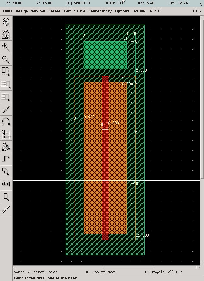
6. Next we need to connect the active regions to metal lines so that they can be routed. The figure below shows the metal1 layer (blue line-shaded polygons) is connected to the active region by an active contact (cc.dg, which is solid black). Remember that the design rule usually restricts the size of the contact to be 2lambda * 2lambda, which is 0.6u * 0.6u. The nselect creates an n+ diffusion in the nwell. This is the body pin of the pmos transistor, which should be connected to power (vdd!). We'll touch on how to connect to the power supply later.
Also, a point of thought usually is how much distance there should be between all these strange looking polygons. That is governed by the design rules, the link for which is given at the website MOSIS Layout Design Rules. You should at least be familiar with some of these rules (e.g. contact size should always be 2 lambda * 2 lambda, distance between poly and active region, etc.). Once you get into the habit of designing manual layouts, you will start to remember the more common design rules. For now, you will have to perform a Design Rule Check (DRC) every now and then on your layout in order to make sure that you have satisfied the rules. More on this can be found on the next page of this online Cadence tutorial.
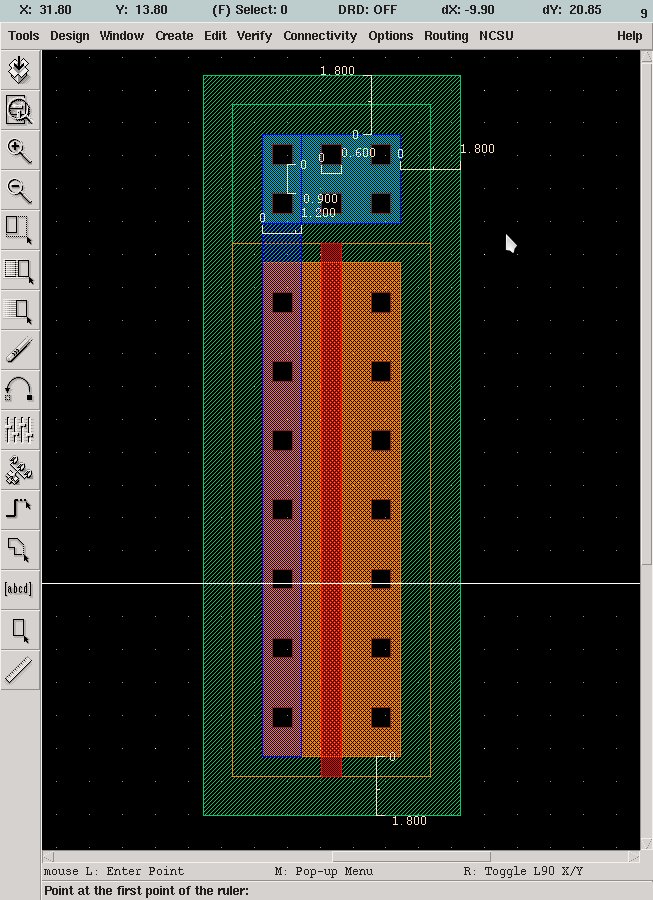
7. Next, you can proceed to create the nmos transistor but this time your nmos needs to be created in the nselect layer while the p+ diffusion of the NMOS is in the pselect. The size of the nmos chosen in this design has the same length as the pmos (0.6um) but the width of the nmos is chosen as 6um instead. Note that since we are using an nwell technology, we don't need an explicit well for the nmos transistor (the pwell) since the background is p-substrate. The figure below shows the inverter.
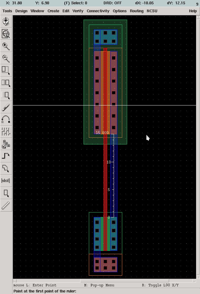
We have chosen to space the nmos and the pmos by the distance of 15um
active-to-active distance for a 0.6um process. This region between the two
transistors would be used for pin definitions and for routing signals from one
layout cell to another. The more the distance between the nmos and the pmos
transistor, the more connections can be routed and less problems to worry about
in the future when designing big cells. However, a large distance may be inefficient
and result in a very big layout. But for the sake of learning, we would rather
choose to go with a large distance of around 15um. Note that you can stretch
the distance between the active layers to make the cell shorter. One way would be to use the s command on the poly and metal1 vertical strip layers
to stretch the layers upwards. You
can then move the rest of the nmos transistor up by highlighting the bottom
portion of the layout with your mouse (all of the edges will be highlighted in
white) and using the m (move) command. Once you are in the move mode, just click once on the highlighted portion
of the layout and move it upwards. Click again to release the selected layers.
A good way to know if you are in the move mode
is to look at the lower left-hand corner of the inverter layout view and read
the messages there. You should see
the following: Select the figure to be moved:
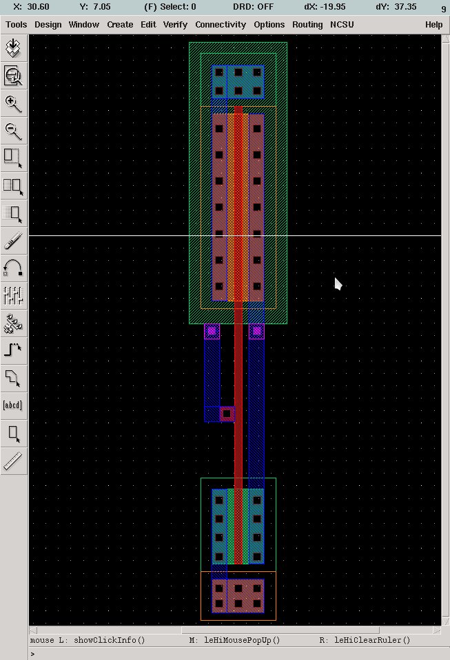
8. The gate of the transistors needs to be connected to the metal1 lines for it to be accessed. To do that you will be using a contact "cc.dg" to make a contact between an already overlapping metal1 and poly layer. Similarly, we desire to then connect the metal1 to metal2 (though it is not necessary) for pin connections. For this purpose, we will make a contact between a metal1 and a metal2 using a "via". There are two ways of doing this.
Method 1: Bring metal1 and metal2 to overlap each other and then draw a "via.dg" rectangle of 2lambda * 2lambda (which is 0.6u*0.6u for AMI 0.6u process). Similarly, bring poly and metal1 together and then draw a "cc.dg" rectangle of 2lambda * 2 lambda.
Method 2: There are some ready-to-use macros available for making contacts. To access a macro cell which has a poly-metal1 combo with a single contact, instantiate the cell " M1_P" (note capital letters) from the library "NCSU_TechLib_ami06". Similarly, to access a metal1-metal2 combo with a via, instantiate the cell "M1_M2" from the NCSU_TechLib_ami06 library. These cells will appear as a black box. To see through the cell, type "Shift -f". This will make the cell visible. Remember that you cannot update this cell, since it is a standard library cell.
The figure below shows the
connection. The red-shaded polygon with a black square at the
center and blue borderline is the M1_P contact. The blue-shaded polygon with a
pink square at the center and pink borderline is the M1_M2 contact.
9. For simulation purposes and standard
cell design rules, it is necessary to add the pin (pn) layer. They are
identical in purpose to the input/output and vdd!/gnd! pins in the schematic
view. Power and ground rail pins should be declared as jumpers.
Input/output pins should be in metal2 while power/ground rail pins should be in
metal1. It would not be a bad idea to label your pins with the text
layer, but make sure to name the labels the same as the pins in your schematic
and put them on top of the labeled wires. Click on metal2.pn in the LSW window.
Then press Ctrl-p in the layout editor window. A window will pop up. Enter the
name 'inp' for labeling input. Choose "Display pin name " option and
define the pin as input. Then click on the left mouse button with the cursor
placed at the top left corner of the metal2 square to be labeled. Then drag the
mouse to the right bottom corner of the same metal2 square to be labeled. Click
one more time inside the metal2 square to place the text. Do the same steps for
placing an "out" pin except for the fact that you declare the pin as
"output".
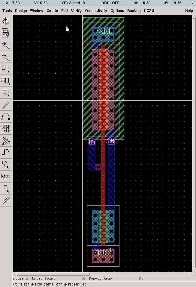
10. Next we want to label the vdd! and gnd! pins. To do this, select the metal1 pn pattern, which is just a blue rectangle outline with an X across. To draw the labels, type Ctrl-P. A pop up menu will appear. Type vdd! for the Terminal Names field and select the I/O type as jumper. Then move your cursor to the starting point of the label and click on the left mouse button. Move your cursor to size the label and click on the left mouse button again. Likewise, label the gnd! pin. The figure below shows the pin labels for vdd! and gnd!
Note that at any time, you can view the
properties of any layout element you placed in your layout view by highlighting
the particular element with the mouse and using the p
(properties) command. This is
especially helpful when you want to identify a particular via or pin that you
have just created.
There are many other useful layout commands and features available through Cadence and most of these options have their own hotkeys. A very good idea would be to take a little bit of time to go through the many layout functions in the menus located at the top of the layout view (eg. Window, Create, Edit, Connectivity, Options) and maybe even try some of them out on your initial layout design. You can always undo your last performed function by clicking on Edit -> Undo or by pressing the u button.
Here are some hotkeys that I have found to be very useful when designing
layouts:
Move about the layout view screen – keyboard arrows (up, down, left, right)
Fit entire layout onto screen – f
Zoom in/out – Ctrl/Shift z
Save design – F2
Cancel previous command – Esc
Reveal all mask layers within each layout cell – Shift f (Use Ctrl f to hide these layers)
Properties – q
Create path – p (Convenient for making interconnections between I/O pins of layout cell; need to select mask layer first from LSW window)
Create rectangle of mask layer – r (Select .dg mask layer first from LSW)
Create pin – Ctrl p (Select .pn mask layer first from LSW)
Instantiate layout cell – i
Select more than one mask layer simultaneously – Hold down Shift and click on each layer (Use Ctrl to deselect a particular layer)
Undo - u
Copy – c
Delete – d
Move – m
Stretch – s (Point to edge of mask layer first using mouse cursor)
Ruler – k (Erase ruler – Shift k)
CONGRATULATIONS!!! You've just created your first inverter, graphically that is....
When working with routing different cells and in the design of bigger cells, please make sure that you pay attention to the following issues:
1. Avoid using polysilicon (poly) as a long wire. Use it only for local, < 6 um, connections since its sheet resistance is quite high (15-30 Ohms/square), as well as its capacitance over field oxide.
2. Use thick wires for power rails, minimum 4 lambda, especially if they are long and supplying a lot of current. Keep in mind that the typical current density rating for metals is 0.5 mA/micron. Size them appropriately for the value of the current they carry.
3. When changing metal layers, the number of contacts to use should follow from the current rating of the contacts themselves. The current density for each contact should be kept below 0.5 mA/micron.
 |
||
| previous | top | next |