Bonding Methods
Updated on 10/14/2014
Contents
1 Direct Wafer Bonding
2 Anodic Wafer Bonding
3 Adhesive Wafer Bonding
4 Glass Frit Wafer Bonding
5 Eutectic Wafer Bonding
6 Transient Liquid Phase (TLP) Wafer Bonding
7 Metal Thermo-compression Wafer bonding
1. Direct Wafer Bonding
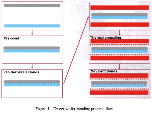
- This is a wafer bonding method in which the adhesion between two surfaces occurs as a result of chemical bonds established between molecules from the two surfaces.
- Typically the adhesion is weak at room temperature (mediated by Van der Waals forces) and maximum bond strength is reached by transforming the weak bonds into covalent bonds through a high temperature thermal annealing (process flow shown in fig. 1).

- For Si-Si direct bonding, the annealing temperature is >600°C for hydrophobic bonding (SiO2 removed from Si prior bonding by 1-2% HF) or >900°C for hydrophilic bonding (with native, thermally grown or deposited oxides). After correct thermal annealing, the bond strength reaches the same range as Si bulk fracture strength.
- Surface activated wafer bonding is also a direct bonding method which uses a special surface preparation process (surface activation) in order to change and control the bonding mechanism by controlling the surface chemistry.
- After surface activation, higher energy bonds are formed at room temperature (even covalent) compared to the nonactivated surfaces and thus the energy required to reach the maximum bond strength by forming covalent bonds across the entire bonded interface is lower.
- As a result, the annealing temperature and annealing time in this case are much lower than in a standard direct bonding process. The annealing temperature for this type of process ranges from room temperature to 400°C, depending on materials to be bonded. The typical surface activation used for this process is a plasma activation using an EVG®800 series plasma chamber for accurate process control.
- Typical materials used for direct wafer bonding under various process conditions are:
- Si, silica, quartz, quartz glass, other glasses (e.g. borofloat, BK7, special properties glasses)
- Compound semiconductors (GaAs, InP, GaP, etc.)
- Oxide materials (LiNbO3, LiTaO3, etc.)
- The general requirement of direct bonding is that surfaces have a microroughness <0.5 nm (in some situations even higher values may be acceptable, depending on process conditions boundaries).
- Microroughness is typically defined as surface Rms measured by Atomic Force Microscope (AFM) on 2 x 2 μm² areas across the substrate.
2. Anodic Wafer Bonding
- Initially reported for joining a metal surface to a glass surface, the term “anodic bonding” is used today mainly to identify the bonding of silicon wafers to glass wafers with high content of alkali oxides (fig. 2).
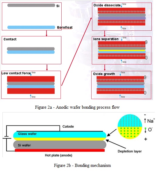
- The glass materials mostly used for anodic bonding are Borofloat from Schott Glass - Germany, and Pyrex7740 from Corning Inc., USA.
- The bond occurs when the two wafers are heated after being brought in contact and an electric field is applied.
- At a certain temperature (depending on the glass composition), oxides dissociate and the mobile alkali ions are driven by the electric field into the glass, creating an oxygen rich layer at the silicon-glass interface. Oxygen ions are driven by the electric field to the silicon surface and produce oxidation of Si. The resulting bond strength is very high and the process is irreversible.
- In terms of equipment, it is important for the bond chamber to provide good temperature uniformity and ensure good electrical contacts.
3. Adhesive Wafer Bonding
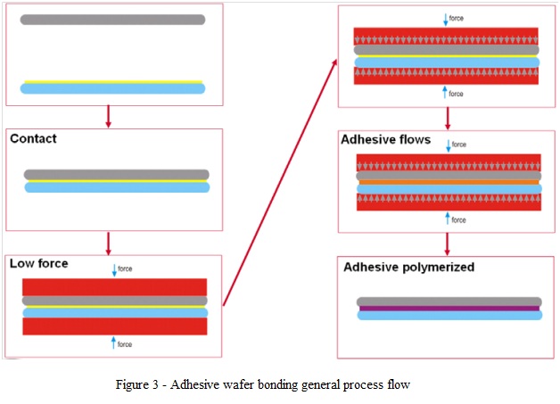
- Adhesive wafer bonding is a technique using an intermediate layer for bonding.
- Polymers, spin-on glasses, resists and polyimides are some of the materials suitable for use as intermediate layers for bonding.
- The choice of the material for intermediate layer is always made considering the substrate materials and topography.
- The main advantages of using this approach are: low temperature processing (maximum temperatures below 400°C), surface planarization and tolerance to particles (the intermediate layer can incorporate particles with the diameter in the layer thickness range).
4. Glass Frit Wafer Bonding
- This type of bond is using as intermediate layer for bonding a low melting point glass.
- The bond occurs by heating the substrates with applied contact force (fig. 4).
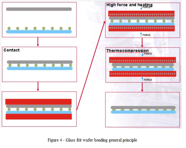
- Glass frit bonding has a high tolerance to surface roughness and can incorporate high topography of the substrates.
- Glass frit material can be deposited by screen printing or used as glass preformed sheets.
- This process is very reliable and is used in high volume production by major MEMS devices manufacturers for applications where low vacuum encapsulation is required.
5. Eutectic Wafer Bonding
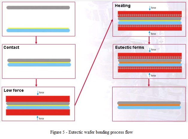
- This is a wafer bonding process which uses as bonding layer an eutectic alloy formed during bond process.
- Eutectic alloy is formed at the bonding interface in a process which goes through a liquid phase: for this reason, eutectic bonding is less sensitive to surface flatness irregularities, scratches, as well as to particles compared to the direct wafer bonding methods (metal layer can incorporate particles with diameter lower than the eutectic layer thickness).
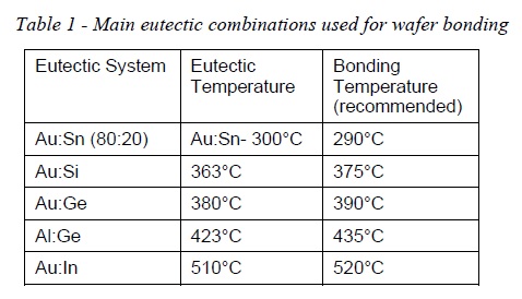
- Some of the main eutectic alloys used for wafer bonding applications are listed in table 1.
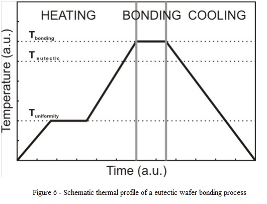
- For a successful eutectic bonding process, it is very important that bonder assures a good temperature uniformity across the entire wafer surface and also to control very well the temperature value (avoid overshooting the set point), in order to have a reliable process.
- Experimental results showed that good quality interfaces are obtained when temperature is raised to a value lower than the eutectic temperature (heating simultaneously from top/bottom), maintained constant for short time to reach uniform heating of both wafers, than increased again by heating both heaters to a temperature exceeding the eutectic point with 10-20°C (depending on specific process conditions and on substrates restrictions) followed by cooling down to a temperature below the eutectic temperature.
- A typical thermal profile of a eutectic wafer bonding process is shown in fig. 6.
- Eutectic wafer bonding does not require application of high contact force.
- Due to the liquid phase formed during the process, high contact force results always in metal squeezing out of the interface, resulting in poor interface layer uniformity as well as contamination of the bond tools and bond chamber.
- The role of the light contact force required is just to ensure good contact of the two wafers and good contact of the two heaters of the bonder with wafers’ back sides.
- Eutectic wafer bonding is a good candidate to high-vacuum applications as this process has a very low specific outgasing due to the use of only high purity components.
- The liquid melt formed during process can only enhance the high vacuum compatibility by allowing high quality sealing even on non-perfect surfaces.
6. Transient Liquid Phase (TLP) Wafer Bonding
- For some applications, the process temperatures must be lower than the bonding temperatures of the most usual eutectic alloys (300°C - 400°C).
- In such situations, an alternative process can be used, which results in an inter-metallic compound bonding layer.
- In literature, this process is known under different names among which can be mentioned “diffusion soldering” or Transient Liquid Phase (TLP) bonding.
- This bonding process is an advanced type of solder bond that can form high-quality hermetic seals at lower temperatures than other bonding technologies.
- This technique uses one thin layer of metal (typically 1-10μm thick) which during a thermal process diffuses into its bonding partner forming an inter-metallic compound layer with re-melting temperature higher than the bonding temperature (table 2). The process flow and recommended thermal profile are the same as for eutectic wafer bonding (fig. 6).
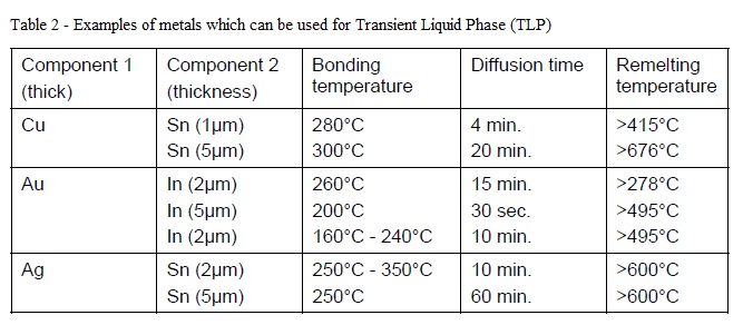
- Table adapted from [G. Humpston, and D. Jacobson, in Principles of Soldering, ASM International 2004, p. 231]. Times correspond to full diffusion of the specified thickness of Component 2.
- Same as eutectic wafer bonding, diffusion soldering bonding is attractive for MEMS vacuum packaging as the process is completed at low temperatures (150°C - 300°C) and can withstand much higher temperatures after bonding (see Table 2), bonding layers are made out of metals (low permeability), and they can planarize over surface defects or particles resulting from prior processes.
7. Metal Thermo-compression Wafer bonding
- Quite often people are wrongly considering that thermo-compression and eutectic bonding are one single process.
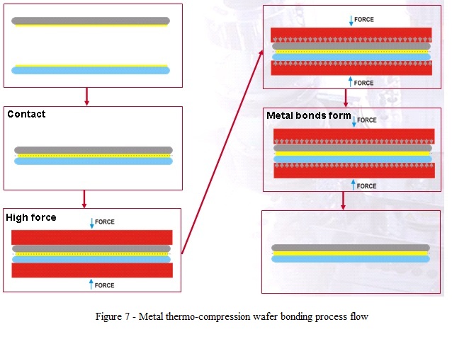
- In thermo-compression bonding process, the two surfaces adhere to each other due to a metal bond established between two metal surfaces pressed together under heating.
- The bonding mechanism is enhanced by the deformation of the two surfaces in contact in order to disrupt any intervening surface films and enable metal-to-metal contact (fig. 7).
- By heating the two metal surfaces, the contact force applied for the bond process can be minimized. High force uniformity across the bonding area results in high yield.
- There are several metals used for metal thermo-compression bonding, as Au, Cu or Al.
- These are considered interesting for wafer bonded MEMS applications mainly due to their availability in main microelectronics applications.
- Their use for one or another type of applications is conditioned by the type of substrates used (e.g. no Aucontaining substrates can be further processed in CMOS lines).
- Typically the metals used for this process are evaporated, sputtered or electroplated on the surface. In such process, it is extremely important to assure a proper diffusion barrier or adhesion layer between the metal bonding layer and its substrate.
- The surface microroughness of the metal bonding layers ranges from <1nm and up to few tens of nm, depending on the metal used, on deposition technique and on the wafer bonding process conditions.
